4B: Thin films of graphite grown on Ni foils by chemical vapor deposition
Abstract
Graphite thin films (GTF) are used as heat-sinks in electronic devices such as mobile phones. Generally, the thickness of these films is in the order of tens of micrometers due to production methods being based on the pyrolysis and graphitization of polymers [1]. As devices scale down, it is important to ensure that thermal management solutions continue to be available which, furthermore, conform to market regulations. Thus, over the past decade, there has been renewed interest in the use of chemical vapor deposition (CVD) to grow sub-micrometer GTF with high structural quality and low surface roughness.
Since the CVD process relies on the thermal dissociation of hydrocarbons onto transition metal substrates, it is important to tailor the catalytic foil to the type of graphite aimed. Due to the relatively high solubility and diffusivity of C into Ni, this metal is commonly preferred for the growth of GTF (as opposed to Cu, the most popular substrate for the growth of single-layer graphene by CVD). To present, there is still little understanding of how to control the production of GTF from Ni foils and if it is possible to achieve wafer-scaled films with less than 100 nm that can be handled without cracking.
In this communication, we will show our recent efforts to produce wafer-scale high-quality GTF with thickness below 100 nm (Fig. 1). Detailed structural analysis of the catalyst-graphite interface and the study of the reactor's parameters permitted valuable insight to the mechanism of GTF formation. Remarkably, regions with just a few layers of graphene were identified (Fig. 1c). Despite this, these films were robust and could be dissociated from the metal foil without the use of a polymer support. After transfer, they retained the expected properties of GTF, added to visible light transparency.
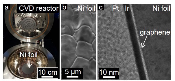
Figure 1: Thermal CVD growth of GTF on Ni foils. (a) Photo of the CVD reactor chamber with a 4" Si wafer where a Ni metal foil was placed; (b) Scanning electron micrograph of the Ni surface with µm-sized grains; (c) Transmission electron micrograph of a post-growth Ni foil, seen in cross-section, where regions with a very thin layer of graphite (graphene) are present. The Pt and Ir originate from the microscopical lamella preparation (by focused ion beam).
References
[1] M. Murakami, K. Watanabe, S. Yoshimura, High-quality pyrographite films, Appl. Phys. Lett., 48 (23), 1594-1596 (1986).
Speakers
Prof. Pedro Da Costa
KAUST, Saudi Arabia